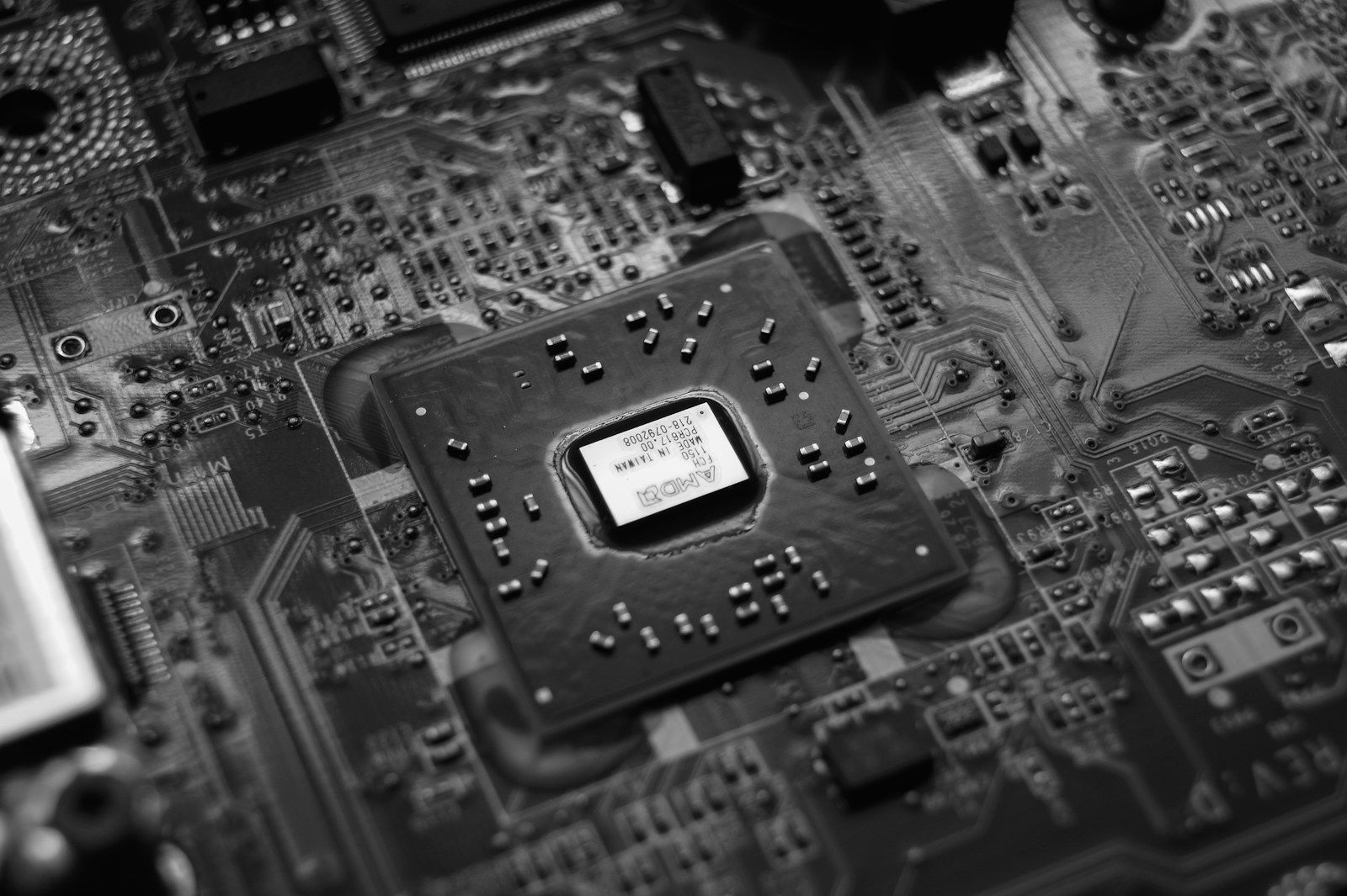
Ever marveled at just how tiny yet effective the chips in your gadgets are? Prepare to marvel some more! Silicon chips are about to be revolutionized, courtesy of our clever tech wizards. As silicon reaches its limit, we’re switching to 2D semiconductors and 3D chip designs to jazz things up. Researchers at the Massachusetts Institute of Technology (MIT) are leading us into this thrilling future of chip technology.
A Matter of Size
Traditional silicon chips require ever-shrinking features to accommodate technology’s growing computational demands. Companies such as Intel and TSMC are busy creating chips with tinier elements. However, there’s a roadblock—the tinier we get, the poorer silicon performs. Currently, the details on our silicon chips are so dense that performance is starting to nosedive. That’s not good news for our tech-loving hearts!
When Silicon Hits the Wall
Here’s the deal. Silicon is a great material for chips, but it has its limits. Push it too hard and it starts to fail. Just like us after a long day of school or work, silicon performs best when it’s not strained to the limits. This has led to a considerable snag in progressing chip tech – but our brilliant scientists at MIT’s Research Laboratory of Electronics are vying an ingenious solution.
Hello, 2D Semiconductors!
While silicon struggles under pressure, a class of materials known as 2D semiconductors aren’t bothered in the least. These graphene-like materials keep on semiconducting, even when we push them down to just one atom in thickness. That’s seriously impressive and exactly what we want in our future tech.
Going 3D: Chip Revolution
3D chips are another way to pack more power into the same space. Instead of shrinking transistor size (like we’ve been doing with silicon), 3D chips achieve higher density by vertically stacking layers of transistors. The result is more working transistors in the same chip area, and increased performance – all without making the transistors any tinier. Clever, right?
Our MIT scientists decided to get the best of both worlds. How? By creating a 3D chip out of stacks of 2D semiconductors! This ground-breaking research may just be the future of chip technology, and a solution to silicon’s limitations.
To Wrap It Up
So, what does all of this mean for us? This simply means our devices could get even slimmer, faster, and more efficient. Thanks to 2D semiconductors and 3D chip designs, we might even enjoy powerful technology microscopic in size!
Emerging tech trends like this exemplify how curiosity and innovation can continually push boundaries, transforming the way we live, learn, and interact with the world. So, the next time you’re playing your favorite game, streaming a viral video, or tapping away on your device, remember: there’s a world of technology specifically designed and tirelessly improved to help you do just that. And it just keeps getting tinier, smarter, and better.
